Tuesday, August 25, 2009

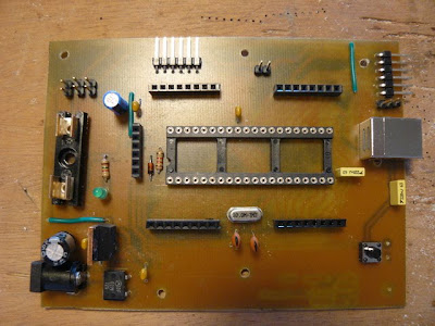
Building Jaluino v1.0

Jaluino, with user guide, schematics, PCB, shields, etc... can now be reached on the following sites:

Main site: http://jaluino.org
Repository: http://jaluino.googlecode.com
Group: http://groups.google.com/group/jaluino


Big time.

Thanks to Richard's last contribution, we now have a nice schematics for the first version of Jaluino board, and very clean and easy to build PCB.

Jaluino is aimed to be a clone of Arduino, but PIC-based, and powered by jalv2 & jallib. The purpose is to share a common hardware configuration, on top of which one can add different features and capabilities, thanks to shields (daughter boards). Ala Arduino...

This post is to give an overview of how to build it, but with not so much details. If you want to build it, you'll have to be familiar with PCB creation.

That said, having this board within your hands is really nice ! It really helps thinking about what could be done with it, what could be improved, and is a nice base to start thinking about building shields.

So, here we go ! First of all, you can find all schematics, PCB and many more details in jallib SVN repository, under "/project/jaluino" directory.

Here's the schematic, but have a look at the PDF file for a more detailed one:


The PCB is surprisingly very simple (thanks Richard !), and thus very to easy to build:


Don't print and use this image ! Use the PDF file here, and print it at scale 1:1, that is, without any zoom-out or zoom-in correction. If any doubt, once printed, put the microcontroller support on the paper (or the like) and check all pins perfectly fit all holes.


PCB creation


As said, PCB creation is easy. I use the toner transfert method, using glossy photo laser paper (dedicated to laser printer, not ink-jet). If interested, have a look at this post, explaining how to do this, step by step, with a video.

Once the transfert is done, the PCB is ready to be etched.


PCB is etched, now drill the holes


PCB is ready for soldering


A brief comparison between original Arduino and Jaluino. Jaluino is obsviously bigger, but embed a much bigger chip, and most importantly is made homebrew!


Soldering components


I try to start soldering components from the smaller & lower ones, to the biggest and taller ones. We'll follow this component diagram, provided in PCB PDF file (page 2).


First solder resistors and diodes


Then solder small capacitors (unpolarized)


Place microcontroller support, quartz, pushbutton and bridge rectifier (I used a DF02M instead of DF04M)


Add wires (green), power jack, big capacitors (polarized)


Solder shield connectors, serial and ICP connects. Add 7805 voltage regulator. Don't forget jumper for power selection and RTS reset feature.


Place USB connector and fuse support


Place your favorite 18F4550 onto the support, and don't forget the fuse ! You're done, kudos !


The reverse side...


Now here's a brief map showing the different features coming with this board.


Note: one important missing feature is I²C support, which surely will come in the next version.

I already tried quite few things with this board: In Circuit Programming using XWisp648, blinking a LED (of course), UART using serial connector, with tinybootloader and testing Reset-via-RTS feature (great), and USB-to-serial ! In the next post, I'll try to describe these experiments one by one.

Another important thing, if not the crucial one, is how big should a shield board must be. Current shield connectors configuration gives a surface closed to Arduino's (only considering the surface between connectors, not the whole board). It it enough ? Should a shield board be bigger ? Now imagine this board is doubled-sided, built through a professional process (and thus available as a commercial product). How much smaller would it be ? Will current connectors configuration be valid ? This is a very important thing, because from this is derived all the shield compatibility. If one builds a shield for this Jaluino v1.0, and shield connectors gets changed, this shield will have to be adapted and rebuilt...

And about shields, now the time has come to design a development shield, providing (more or less) basic features. This shield could be used to learn jalv2 & jallib. I was thinking about having:
  • one LED connected to a standard digital output
  • one LED connected to a PWM channel
  • maybe a buzzer connected to the other PWM channel to make sounds
  • one or two push-buttons (input)
  • pot to have fun with ADC
  • maybe an EEPROM to play with I²C
  • a small LCD screen (8x2)
But maybe that's a little bit too much for single shield...


Please advise !


Sébastien Lelong & Richard Zengerink.

Monday, August 10, 2009

PIC 18f14k50 based USB WISP programmer

Introduction
Today the description of a USB WISP programmer. A while back I had some trouble with my ICD2 clone, therefore I decided to make a WISP programmer. Since I've written the USB libraries for JAL(lib) and because I just had ordered a tube of 10 PIC18f14k50, I decided to redesign the original WISP so it uses the PIC18f instead of the the PIC16f648 (which I did not have in my junk box), and use the USB-Serial library so I can still use the various host applications but I can plug it in directly to the USB port. The additional benifits are:

  • Very cheap (just a PIC18f14k50 + resistor and capacitors, total costs ~5 Euro)
  • Have a fast serial connection
  • Can use exsisting WISP host applications (like Rob's XWISP2)
  • Can be directly powered from the USB port (no external power supply needed)
  • When adding a 3.3V regulator, board can also be used to program LF devices (if Vpp = 9v)
  • Added an additional connector for future use, like JTAG & I2C and RS-232 TTL

The schematic is very straigtforward, the blue boxed areas contain the optional section of the USB WISP programmer


I've made a few modifications to the original design, first the Target power is controlled by a PNP transistor, which acts as switch (so target power can be turned on/off), because USB 5v does not like to be short circuited for a short period, as is done in the WISP 648. In addition I've added a PNP transistor to control the Target VPP line, this is for future use.

I also made a small PCB, however, Wouter van Ooijen (the designer of the Wisp 648 programmer, see www.voti.nl) asked me not to publish the PCB layout. So don't ask me for it, if you want to build this project you have to design you own PCB, if you can't, buy a Wisp 648 kit from Wouter. The assembled PCB is depicted below:


The Source code
I just made minor modifications to the original source code (see www.voti.nl). The changes are:
  • Include usb_serial library
  • Change UART functions, so they send and receive chars from the USB library
  • Tune the timing delays (becuase effective speed is raised from 20->48 MHz)
  • Had to adapt the HEX<->ASCII function, because the original code still uses some inline assembly which did not work properly for the PIC18f
  • Call USB-Flush in the main routing

There still some work left, i.e. the port trough function is not working yet, the advantage of this design is the the UART can be used (even the polarity inversion of the UART signals can be programmed with the PIC18f14k50), so pass trough can work with speeds up to 115200 baud.
The JAL source code is uploaded in the JALLIB google code file download section, http://groups.google.com/group/jallib/files

Results
The USB Wisp is operation for a couple of weeks, so far it worked flawlessly. With a small change in the XWISP2 configuration file, I was able to program the PIC14k50 as well. But of course, there is a big discalaimer, I only have a couple of PICs, so the solution is not tested extensivly, thus if you want a good and robust PIC programmer I advice you to buy or build the original WISP 648.

Conclusion
This small exerise shows the strenght(s) of JalV2 and Jallib, it shows how easy it is to port a large application from a PIC16f devices to a PIC18f device and that only a little effort is required to move from a RS-232 (UART) communcation interface to a USB (serial) based communication interface.


Sunday, August 2, 2009

Jaluino Medium 18F2550-based: first draft


Jaluino, with user guide, schematics, PCB, shields, etc... can now be reached on the following sites:

Main site: http://jaluino.org
Repository: http://jaluino.googlecode.com
Group: http://groups.google.com/group/jaluino


Careful, schematic and PCB in this post aren't tested yet. Except if you're a daring risk-taker, you shouldn't build this board as it would only be a waste of time, and probably of money too... You've been warned.

I'm still on this Jaluino board.

While trying to get a working schematic, I've also spend a lot of time drawing the PCB. I focused on a 18F2550 version, instead of big fat 18F4550, so PCB layout is simpler and I can focus more important issues for now. So this is now about Jaluino Medium (18F2550), not Jaluino Maxi (18F4550). BTW any ideas about "marketing" names to replace Mini, Medium and Maxi ?...

Last schematic contained lots of errors, mostly on USB and dual power. Luckily Guru Albert helped and provided me four options. I kept the simpler one (I can understand), which consists in having a jumper to select whether power should come from:
  • external supply (jack)
  • USB self-powered connector
(I would even add a new source of power: from serial, and more specifically from a USB-to-serial converter)

The current schematic seems to look better (yet still untested, this will be for other posts).


So here how the PCB looks like now...


This PCB is expected to be 8.1cm x 7.1cm (3.2in x 2.81in). Compared to an original Arduino (6.9cm x 5.4cm), it's a little bit bigger. But it's also a single side board, and there are lots of other connectors (I²C and serial) not present in Arduino.

There are several connectors. Some will be the shield connectors (JP1, JP2, JP4, JP5 and POWER), female headers as in Arduino, others (ICSP/JP6, I²C, serial) will be male headers.

The shield is expected to be something like 4.8cm x 5.8cm (1.9in x 2.3in). Original Arduino's shield is 4.9cm x 4.3cm. It's a little bit bigger, and I may adjust connectors (move JP1 & JP2 lower) to have a "more squared shape".


Next posts will be about testing and prototyping this board, using a breadboard. This will also be a good exercise to have basic (and maybe advanced) experiments using jalv2 and jallib.


Sébastien Lelong